High-Precision Explosion-Proof Platform Scales: Empowering Korean Semiconductor Partners to Break Through Production Constraints

In the field of semiconductor manufacturing, precision and safety are the key anchors for building a solid production foundation. Microtess deeply understands the industry’s needs and has created customized high-precision explosion-proof platform scales for Korean semiconductor partners, accurately solving production challenges and injecting reliable momentum into advanced wafer packaging and testing operations.

picture

I. Customer Background: “Precise” Needs in Semiconductor Manufacturing

Our partner, a semiconductor manufacturer in Korea specializing in advanced wafer packaging and testing, features a production line with high automation, high cleanliness, and strict requirements. In processes involving the handling of special gases, weighing of tiny chip components, and containers of corrosive chemicals, the explosion-proof performance, space adaptability, and precision control of equipment are extremely stringent. Traditional scales fall short, becoming bottlenecks restricting production efficiency and safety.

II. Core Challenges: Stringent Requirements Across Dimensions

(1) Precision and Stability Dilemma

Weighing tiny chip components demands extreme precision. Even minor fluctuations in the workshop’s constant temperature environment can affect packaging yields due to scale zero drift, making precision and stability control critical.

(2) Explosion-Proof and Safety Compliance Barriers

Production involves flammable and explosive gases and corrosive chemicals. Explosion-proof certification for hazardous areas and equipment corrosion resistance are mandatory for ensuring safety, leaving no room for compromise.

(3) Space and Automation Adaptation Challenges

The compact production line layout requires scales to fit precisely with robotic arms and conveyor tracks for seamless automation. The “rigid” dimensions of traditional standard scales cannot adapt.

(4) Cleanroom Compatibility Requirements

A high-cleanliness workshop environment demands scale surfaces without pores or grooves, resistant to frequent cleaning, and free from particle contamination of wafers, imposing special requirements on equipment materials and structural design.

picture

III. Microtess Custom Solutions: Accurately Solving Problems

(1) Precision and Structural Optimization: Building a “Precise” Foundation

  • Sensor and Algorithm Synergy: Utilizes high-precision strain gauge sensors with customized instruments for excellent resolution. Incorporates a built-in air pressure compensation module to counter micro-environmental fluctuations, ensuring stable and accurate readings for reliable weighing of chip components.
  • Mechanical Structure Enhancement: Adds shock-absorbing buffers to the scale base to absorb high-frequency vibrations (vibration transmission rate < 1%). The housing is integrally formed from 316L stainless steel with electrochemical polishing (Ra < 0.8μm), enhancing corrosion resistance and reducing particle adhesion, establishing a dual-dimensional precision guarantee system.

(2) Explosion-Proof and Material Innovation: Building a Safety Barrier

  • Explosion-Proof Design: The 316L stainless steel housing is laser-welded and sealed to IP66, filled with inert gas (nitrogen) to isolate flammable gases from circuits. Uses intrinsically safe circuits (Ex ia IIC T4) with explosion-proof certified components, ensuring no sparks and preventing internal faults from causing explosions.
  • Corrosion Resistance Upgrade: The scale platform and sensor housing use PTFE coating (0.2 – 0.5mm thick) via plasma spraying, withstanding strong acids and alkalis. Accelerated life tests show a wear rate < 5%, extending equipment life by 3 times compared to traditional solutions.

(3) Space Customization Design: “Flexible Integration” for Compact Production Lines

  • Precise Size Reduction: Strictly following the production line layout, the scale dimensions are compressed to 30cm (W) × 25cm (D) × 11cm (H), with M6 threaded positioning holes for robotic arm integration. Supports SMEMA protocol for seamless automation, eliminating manual intervention.
  • Installation Without Modification: Modular quick-install design fits directly into pre-reserved slots, completing mechanical installation and circuit debugging within 2 hours without altering existing production lines, enabling “plug-and-play.”

(4) Cleanliness and Compliance Details: Meeting Cleanroom Standards

  1. No-Dead-Corner Clean Structure: Laser welding and rounded transitions eliminate dust traps, ensuring easy cleaning with cleanroom mops. Cables use anti-fall connectors and PFA hoses for low volatility and corrosion resistance.

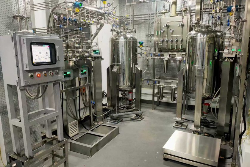
Low Volatility and Anti-Static Properties: All non-metallic parts meet SEMI C12 certification, ensuring VOC emissions < 0.05mg/m³ under high-temperature cleaning. The housing features anti-static treatment (surface resistance 10^7 Ω), preventing particle adhesion and ESD damage to chips.

IV. Implementation Results: A “Practical” Witness to Production Line Renewal

(1) Precision Drives Yield Improvement: From “Trial-and-Error” to “Precision”

After deployment, the weighing error of chip components reduced from ±0.5mg to ±0.03mg, improving packaging yield by 2.3%. In a production batch of 100,000 chips, it directly reduced 2,300 defective reworks, saving approximately $120,000 (including materials, labor, and testing costs).
Real-time data upload via MES enables “defective product tracing,” reducing problem time from 4 hours to 30 minutes.

(2) Efficiency Drives Production Speed: From “Bottlenecks” to “Smooth Flow”

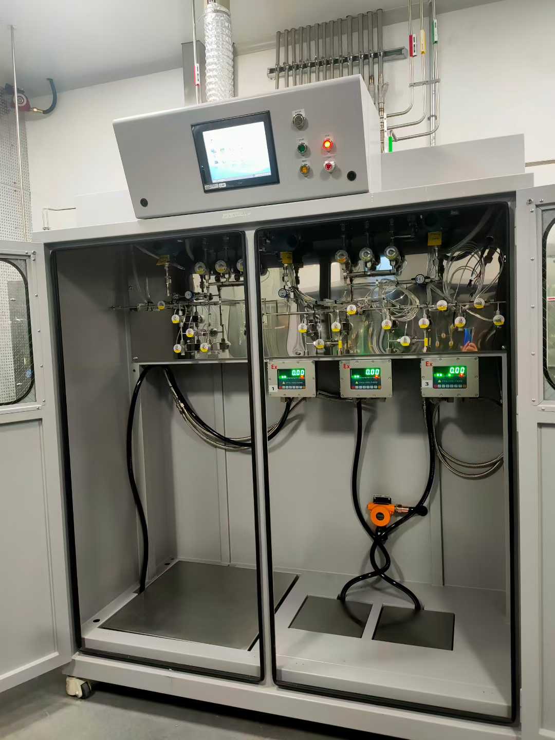
The compact design integrates seamlessly into the production line, reducing the weighing time per batch (500 chip components) from 8 minutes to 3 minutes, increasing daily throughput by 167% (from 1,200 to 3,200 units).
Robotic arm operators report: “The equipment now runs continuously for 8 hours, increasing ‘lights-out production’ from 30% to 70%, significantly improving efficiency.”

(3) Safety Ensures Stable Production: From “Hazards” to “Peace of Mind”

With explosion-proof and corrosion-resistant designs, the scales eliminate risks of chemical leaks and gas explosions (passing the Korean KCs safety audit). In accidental hydrofluoric acid leakage tests, the PTFE coating effectively resists corrosion, ensuring stable operation.
Customer Production Director’s Comment:
“Microtess’s customized solution redefines our understanding of ‘industrial scales’—it’s not just a weighing tool but a link connecting precision, efficiency, and safety. Every detail reflects a deep understanding of semiconductor manufacturing, solving current problems and preparing for future 3nm packaging processes.”
picture

V. About Microtess: Customization Expert in Semiconductor Deep Cultivation

In the semiconductor precision manufacturing field, Microtess understands that “standards” cannot meet “precise” needs. We use “scenario deconstruction + technological innovation + compliance implementation” to create customized solutions:
  • Whether your semiconductor production line faces cleanroom adaptation, explosion-proof compliance, or micro-precision weighing challenges, Microtess provides tailored solutions.
  • Contact us now and let Microtess be your production problem solver, defining new possibilities in semiconductor manufacturing with customized precision.
  • Scenario Deconstruction: Deeply analyze production line layouts, airflows, and operational habits to ensure solutions fit real needs.
  • Technological Innovation: Integrate sensor miniaturization, explosion-proof materials, and intelligent algorithms to break performance boundaries.
  • Compliance Implementation: Adhere to international standards (SEMI, ATEX, IECEx) to avoid market access risks.
Whether your semiconductor production line faces cleanroom adaptation, explosion-proof compliance, or micro-precision weighing challenges, Microtess provides tailored solutions.
 

Contact Now

    Contact Now

      CHOOSE YOUR LANGUAGE

      Contact Now